31 31b-PrimeDetector
31 : 31b-PrimeDetector
- Author: Aidan McNay
- Description: Detects whether a 31-bit number is prime or not
- GitHub repository
- Clock: 0 Hz
How it works
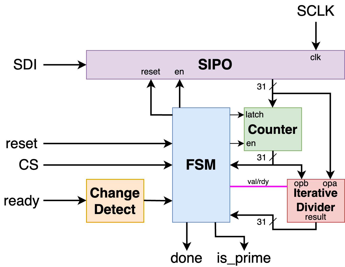
The 31-bit Prime Detector takes in a 31-bit number (shifted in serially). Once the number is obtained, the FSM control logic takes over. It attempts to divide the value by all numbers less than it; if it finds one that divides evenly, the logic stops and declares the number not prime. If it doesn't divide evenly by any of these, the number is declared prime.
Due to space constraints, the design uses an iterative divider and FSM logic to minimize space usage. Further information can be taken from the README.md on the GitHub page
How to test
This design requires an external clock. Before testing, the design should be reset with the appropriate pin (active high), which resets the stored value to 0. To shift in a value, use the SPI-like interface; when the CS line is enabled (active low), on rising edges of SCLK, the data present at SDI is shifted in. Data is shifted into the LSB, and progressively shifted to more significant bits as new data is received (with the data at MSB being shifted out and disregarded).
Once you have the desired number stored, start the calculations by enabling the ready pin (active high). Note that the stored value cannot change while calculations are ongoing.
Once the calculations are finished, the done pin will be driven high. The result will be shown on the is_prime pin; a value of 1 indicates that the value inputted is prime.
External hardware
External Clock, 5 buttons for inputs, 2 LEDs for outputs

IO
| # | Input | Output |
|---|---|---|
| 0 | clock | done |
| 1 | reset | is_prime |
| 2 | SDI | waiting |
| 3 | SCLK | GND |
| 4 | CS | GND |
| 5 | ready | GND |
| 6 | NC | GND |
| 7 | NC | GND |