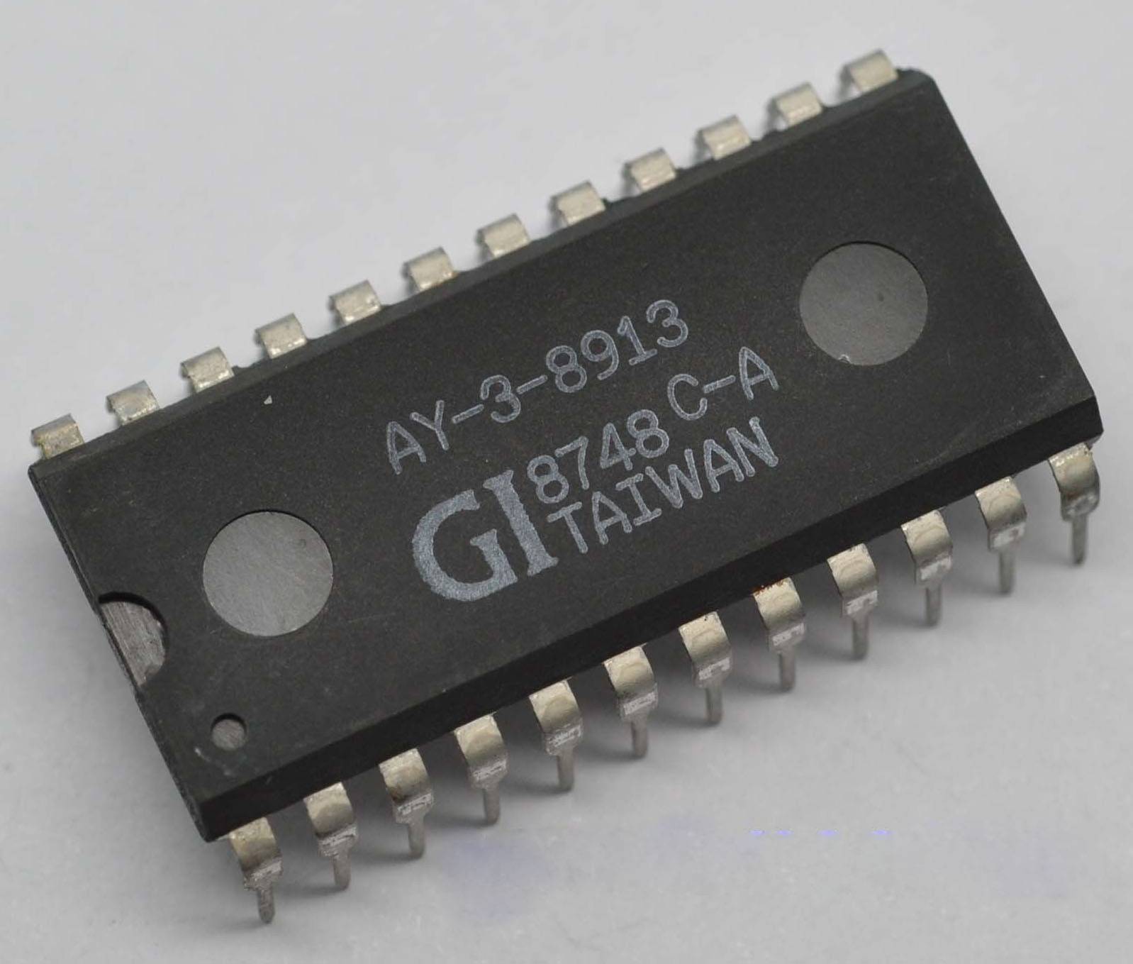
165 Classic 8-bit era Programmable Sound Generator AY-3-8913
165 : Classic 8-bit era Programmable Sound Generator AY-3-8913
- Author: ReJ aka Renaldas Zioma
- Description: The AY-3-8913 is a 3-voice programmable sound generator (PSG) chip from General Instruments. The AY-3-8913 is a smaller variant of AY-3-8910 or its analog YM2149.
- GitHub repository
- Clock: 2000000 Hz
How it works
This Verilog implementation is a replica of the classical AY-3-8913 programmable sound generator. With roughly a 1500 logic gates this design fits on a single tile of the TinyTapeout.
The goals of this project
- closely replicate the behavior and eventually the complete design of the original AY-3-891x with builtin DACs
- provide a readable and well documented code for educational and hardware preservation purposes
- leverage the modern fabrication process
A significant effort was put into a thorough test suite for regression testing and validation against the original chip behavior.
Chip technical capabilities
- 3 square wave tone generators
- A single white noise generator
- A single envelope generator able to produce 10 different shapes
- Chip is capable to produce a range of waves from a 30 Hz to 125 kHz, defined by 12-bit registers.
- 16 different volume levels
Registers The behavior of the AY-3-891x is defined by 14 registers.
| Register | Bits used | Function | Description |
|---|---|---|---|
| 0 | xxxxxxxx |
Channel A Tone | 8-bit fine frequency |
| 1 | ....xxxx |
---//--- | 4-bit coarse frequency |
| 2 | xxxxxxxx |
Channel B Tone | 8-bit fine frequency |
| 3 | ....xxxx |
---//--- | 4-bit coarse frequency |
| 4 | xxxxxxxx |
Channel C Tone | 8-bit fine frequency |
| 5 | ....xxxx |
---//--- | 4-bit coarse frequency |
| 6 | ...xxxxx |
Noise | 5-bit noise frequency |
| 7 | ..CBACBA |
Mixer | Tone and/or Noise per channel |
| 8 | ...xxxxx |
Channel A Volume | Envelope enable or 4-bit amplitude |
| 9 | ...xxxxx |
Channel B Volume | Envelope enable or 4-bit amplitude |
| 10 | ...xxxxx |
Channel C Volume | Envelope enable or 4-bit amplitude |
| 11 | xxxxxxxx |
Envelope | 8-bit fine frequency |
| 12 | xxxxxxxx |
---//--- | 8-bit coarse frequency |
| 13 | ....xxxx |
Envelope Shape | 4-bit shape control |
Square wave tone generators Square waves are produced by counting down the 12-bit counters. Counter counts up from 0. Once the corresponsding register value is reached, counter is reset and the output bit of the channel is flipped producing square waves.
Noise generator Noise is produced with 17-bit Linear-feedback Shift Register (LFSR) that flips the output bit pseudo randomly. The shift rate of the LFSR register is controller by the 5-bit counter.
Envelope The envelope shape is controlled with 4-bit register, but can take only 10 distinct patterns. The speed of the envelope is controlled with 16-bit counter. Only a single envelope is produced that can be shared by any combination of the channels.
Volume Each of the three AY-3-891x channels have dedicated DAC that converts 16 levels of volume to analog output. Volume levels are 3 dB apart in AY-3-891x.
Historical use of the AY-3-891x
The AY-3-891x family of programmable sound generators was introduced by General Instrument in 1978. Soon Yamaha Corporation licensed and released a very similar chip under YM2149 name.
Both variants of the AY-3-891x and YM2149 were broadly used in home computers, game consoles and arcade machines in the early 80ies.
- home computers: Apple II Mockingboard sound card, Amstrad CPC, Atari ST, Oric-1, Sharp X1, MSX, ZX Spectrum 128/+2/+3
- game consoles: Intellivision, Vectrex, Amstrad GX4000
- arcade machines: Frogger, 1942, Spy Hunter and etc.
The AY-3-891x chip family competed with the similar Texas Instruments SN76489.
The original pinout of the AY-3-8913
The AY-3-8913 was a 24-pin package release of the AY-3-8910 with a number of internal pins left simply unconnected. The goal of AY-3-8913 was to reduce complexity for the designer and reduce the foot print on the PCB. Otherwise the functionality of the chip is identical to AY-3-8910 and AY-3-8912.
             ,--._.--.
      GND ---|1    24|<-- /cs*
     BDIR -->|2    23|<--  a8*
      BC1 -->|3    22|<-- /a9*
      DA7 <->|4    21|<-- /RESET
      DA6 <->|5    20|<-- CLOCK
      DA5 <->|6    19|--- GND
      DA4 <->|7    18|--> CHANNEL C OUT
      DA3 <->|8    17|--> CHANNEL A OUT
      DA2 <->|9    16|    not connected
      DA1 <->|10   15|--> CHANNEL B OUT
      DA0 <->|11   14|<-- test*
    test* <--|12   13|<-- VCC
             `-------'
      * -- omitted from this Verilog implementation
Difference from the original hardware
This Verilog implementation is a completely digital and synchronous design that differs from the original AY-3-8913 design which incorporated internal DACs and analog outputs.
Audio signal output While the original chip had no summation The module provides two alternative outputs for the generated audio signal:
- digital 8-bit audio output suitable for external Digital to Analog Converter (DAC)
- pseudo analog output through Pulse Width Modulation (PWM)
Master output channel In contrast to the original chip which had only separate channel outputs, this implementation also provides an optional summation of the channels into a single master output.
No DC offset This implementation produces output 0/1 waveforms without DC offset.
No /A8, A9 and /CS pins The combination of /A8, A9 and /CS pins orginially were intended to select a specific sound chip out the larger array of devices connected to the same bus. In this implementation this mechanism is omitted for simplicity, /A8, A9 and /CS are considered to be tied low and chip behaves as always enabled.
Synchronous reset and single phase clock The original design employed 2 phases of the clock and asynchronous reset mechanism for operation of the registers.
To make it easier to synthesize and test on FPGAs this implementation uses single clock phase and synchronous reset for registers.
The reverse engineered AY-3-891x
This implementation would not be possible without the reverse engineered schematics and analysis based on decapped AY-3-8910 and AY-3-8914 chips.
How to test
The data bus of the AY-3-8913 chip has to be connected to microcontroller and receive a regular stream of commands. The AY-3-8913 produces audio output and has to be connected to a speaker. There are several ways how the overall schematics can be established.
8-bit parallel output via DAC One option is to connect off the shelf data parallel Digital to Analog Converter (DAC) for example Digilent R2R Pmod to the output pins and route the resulting analog audio to piezo speaker or amplifier.
  uController             AY-3-8913
  ,---------.            ,---._.---.
  |         |    2 Mhz ->|CLK  SEL0|<-- 0
  |    GPIOx|----------->|BC1  SEL1|<-- 0
  |    GPIOx|----------->|BDI      |         ,----------.
  |    GPIOx|----------->|DA0  OUT0|-------->|LSB       |
  |    GPIOx|----------->|DA1  OUT1|-------->|          |
  |    GPIOx|----------->|DA2  OUT2|-------->|   pDAC   |  Headphones
  |    GPIOx|----------->|DA3  OUT3|-------->|    or    |      or
  |    GPIOx|----------->|DA4  OUT4|-------->| RESISTOR |    Buzzer
  |    GPIOx|----------->|DA5  OUT5|-------->|  ladder  |         /|
  |    GPIOx|----------->|DA6  OUT6|-------->|          |     .--/ |
  |    GPIOx|----------->|DA7  OUT7|-------->|MSB       |-----|    |
  `---------'            `---------'         `----------'     `--` |
                                                               |  `|
                                                               |
                                                          GND ---
AUDIO OUT through RC filter Another option is to use the Pulse Width Modulated (PWM) AUDIO OUT pin that combines 4 channels with the Resistor-Capacitor based low-pass filter or better the Operation Amplifier (Op-amp) & Capacitor based integrator:
  uController             AY-3-8913
  ,---------.            ,---._.---.
  |         |    2 Mhz ->|CLK  SEL0|<-- 0
  |    GPIOx|----------->|BC1  SEL1|<-- 0
  |    GPIOx|----------->|BDIR     |
  |    GPIOx|----------->|DA0      |
  |    GPIOx|----------->|DA1      |
  |    GPIOx|----------->|DA2      |          C1
  |    GPIOx|----------->|DA3      |     ,----||----.
  |    GPIOx|----------->|DA4      |     |          |
  |    GPIOx|----------->|DA5      |     |  Op-amp  |        Speaker
  |    GPIOx|----------->|DA6 AUDIO|     |   |X     |            /|
  |    GPIOx|----------->|DA7  OUT |-----+---|-X    |   C2   .--/ |
  `---------'            `---------'         |  }---+---||---|    |
                                          ,--|+/             `--` |
                                          |  |/               |  `|
                                          |                   |
                                     GND ---             GND ---
Separate channels through the Op-amp The third option is to externally combine 4 channels with the Operational Amplifier and low-pass filter:
  uController             AY-3-8913
  ,---------.            ,---._.---.
  |         |    2 Mhz ->|CLK  SEL0|<-- 0
  |    GPIOx|----------->|BC1  SEL1|<-- 0
  |    GPIOx|----------->|BDIR     |
  |    GPIOx|----------->|DA0      |
  |    GPIOx|----------->|DA1      |
  |    GPIOx|----------->|DA2      |           C1
  |    GPIOx|----------->|DA3      |      ,----||----.
  |    GPIOx|----------->|DA4      |      |          |
  |    GPIOx|----------->|DA5     A|---.  |  Op-amp  |        Speaker
  |    GPIOx|----------->|DA6     B|---+  |   |X     |            /|
  |    GPIOx|----------->|DA7     C|---+--+---|-X    |   C2   .--/ |
  `---------'            `---------'          |  }---+---||---|    |
                                           ,--|+/             `--` |
                                           |  |/               |  `|
                                           |                   |
                                      GND ---             GND ---
Summary of commands to communicate with the chip
The AY-3-8913 is programmed by updating its internal registers via the data bus. Below is a short summary of the communication protocol of AY-3-891x. Please consult AY-3-891x Technical Manual for more information.
| BDIR | BC1 | Bus state description |
|---|---|---|
| 0 | 0 | Bus is inactive |
| 0 | 1 | (Not implemented) |
| 1 | 0 | Write bus value to the previously latched register # |
| 1 | 1 | Latch bus value as the destination register # |
Latch register address First, put the destination register adress on the bus of the chip and latch it by pulling both BDIR and BC1 pins high.
Write data to register Put the desired value on the bus of the chip. Pull BC1 pin low while keeping BDIR pin high to write the value of the bus to the latched register address.
Inactivate bus by pulling both BDIR and BC1 pins low.
| Register | Format | Description | Parameters |
|---|---|---|---|
| 0,2,4 | ffffffff |
A/B/C tone period | f - low bits |
| 1,3,5 | 0000FFFF |
---//--- | F - high bits |
| 6 | 000fffff |
Noise period | f - noise period |
| 7 | 00CBAcba |
Noise / tone per channel | CBA - noise off, |
cba - tone off |
|||
| 8,9,10 | 000Evvvv |
A/B/C volume | E - envelope on, |
v - volume level |
|||
| 11 | ffffffff |
Envelope period | f - low bits |
| 12 | FFFFFFFF |
---//--- | F - high bits |
| 13 | 0000caAh |
Envelope Shape | c - continue, a - attack, A - alternate, h - hold |
Note frequency
Use the following formula to calculate the 12-bit period value for a particular note:
$ tone period_{cycles} = clock_{frequency} / (16_{cycles} * note_{frequency}) $
For example 12-bit period that plays 440 Hz note on a chip clocked at 2 MHz would be:
$ tone period_{cycles} = 2000000 Hz / (16_{cycles} * 440 Hz) = 284 = 11C_{hex} $
An example to play a note at a maximum volume
| BDIR | BC1 | DA7..DA0 | Explanation |
|---|---|---|---|
| 1 | 1 | xxxx0000 |
Latch tone A coarse register address $0 = 0000_{bin}$ |
| 1 | 0 | xxxx0001 |
Write high 4-bits of the 440 Hz note $1 = 0001_{bin}$ |
| 1 | 1 | xxxx0001 |
Latch tone A fine register address $1_{dec} = 0001_{bin}$ |
| 1 | 0 | 00011100 |
Write low 8-bits of the note $1C_{hex} = 00011100_{bin}$ |
| 1 | 1 | xxxx1000 |
Latch channel A volume register address $8 = 1000_{bin}$ |
| 1 | 0 | xxx01111 |
Write maximum volume level $15_{dec} = 1111_{bin}$ with the envelope disabled |
Timing diagram

CLK   ____      ____      ____      ____      ____      ____
   __/    `____/    `____/    `____/    `____/    `____/    `____ ...
    |         |         |         |         |         |
    |         |         |         |         |         |

BDIR ______    ______    ______    ______    ______    ______
   _/      `__/      `__/      `__/      `__/      `__/      `__

BC1  _______             _______            ________
   _/       `___________/       `__________/        `___________

DA7..DA0_____  ________  ________  ________  ________  ________
   _/  0000  `/xxxx0001`/  0001  `/00011100`/  1000  `/xxx01111`
      latch     write     latch      write    latch
Externally configurable clock divider
| SEL1 | SEL0 | Description | Clock frequency |
|---|---|---|---|
| 0 | 0 | Standard mode, clock divided by 8 | 1.7 .. 2.0 MHz |
| 1 | 1 | -----//----- | 1.7 .. 2.0 MHz |
| 0 | 1 | New mode for TT05, no clock divider | 250 .. 500 kHZ |
| 1 | 0 | New mode for TT05, clock div. 128 | 25 .. 50 MHz |
| SEL1 | SEL0 | Formula to calculate the 12-bit tone period value for a note |
|---|---|---|
| 0 | 0 | $clock_{frequency} / (16_{cycles} * note_{frequency})$ |
| 1 | 1 | -----//----- |
| 0 | 1 | $clock_{frequency} / (2_{cycles} * note_{frequency})$ |
| 1 | 0 | $clock_{frequency} / (128_{cycles} * note_{frequency})$ |
External hardware
DAC (for ex. Digilent R2R PMOD), RC filter, amplifier, speaker
IO
| # | Input | Output | Bidirectional |
|---|---|---|---|
| 0 | DA0 - multiplexed data/address bus | audio out (pwm) | (in) **BC1** bus control |
| 1 | DA1 - multiplexed data/address bus | digita audio least significant bit | (in) **BDIR** bus direction |
| 2 | DA2 - multiplexed data/address bus | digita audio | (in) **SEL0** clock divider |
| 3 | DA3 - multiplexed data/address bus | digita audio | (in) **SEL1** clock divider |
| 4 | DA4 - multiplexed data/address bus | digita audio | (out) channel A (PWM) |
| 5 | DA5 - multiplexed data/address bus | digita audio | (out) channel B (PWM) |
| 6 | DA6 - multiplexed data/address bus | digita audio | (out) channel C (PWM) |
| 7 | DA7 - multiplexed data/address bus | digita audio most significant bit | (out) AUDIO OUT master (PWM) |